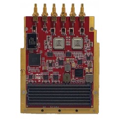


FMCP-DAC12p0 is a 4 channels DAC module based on the industry-standard Vita57.4 FMC+ standard. It utilizes 2 AD9172 onboard for Digital to Analog Conversion and interfaces work through the JESD204B IP core. It samples with 16 bits at 12.0 GS/s.
FMCP-DAC12p0 is a four channels DAC module based on the industry-standard FMC+ standard. It utilizes two onboard AD9172 for Digital to Analog Conversion, and interfaces work through the JESD204B IP core. This module is an advanced High-speed Digital to Analog converter in the market with a 16-bit resolution capable of a sample rate at 12.6 GSPS and has dual channels in a single package. Each DAC IC can be configured via the SPI interface separately.
The module includes an HMC7044 – High-performance 3.2GHz JESD204B jitter attenuator for obtaining the best results. Onboard the module is a 100 MHz onboard VCXO; and 10 MHz TCXO as reference clock, or external user reference clock;
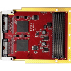
To maximize utilization of FPGA carrier card transceivers, FMCP-DAC12p0 has a carrier-type FMC+ connector on the solder side. So an FMCP-ADC3p0 can be piggy-backed by this module which means, all 16 Rx and TX transceivers of carrier cards can be used. This feature is the optimization of transceivers’ use offered by this module. On 1 FMC+ site, a four-channel DAC and a four-channel ADC can coexist and provide substantial savings in space and resource use.
Features
Applications
IP Cores/Drivers/BSP:
Ordering Information:
Please sign in first.
Sign inCreate a free account to use wishlists.
Sign in